
From the HOD’s Desk……

Role of NBA Accreditation
As we are moving through the different phases of NBA Accreditation process for our institution, I would like to use this opportunity to emphasize on the need, impacts, significance and benefits of this accreditation system. Through this process, the characteristics of our Institution and its programmes will be assessed against a set of criteria established by National Board of Accreditation. NBA provides a quality seal or label that differentiates the Institutions from its peers at the national level. This leads to a widespread recognition and greater appreciation of the Institution’s brand name and motivates it to strive for more.
Beyond quality assurance of an Institution/programme, accreditation system also encourages their quality improvement initiatives, improves student enrollment both in terms of quality and quantity, helps the Institution in securing necessary funds, enhances employability of graduates, facilitates transnational recognition of degrees and mobility of graduates and professionals. It also helps to create sound and challenging academic environment in the Institution, and contributes to social and economic development of the country by producing high quality technical manpower.
By undergoing this accreditation process, we ensure that our Institution’s systems and procedures get aligned with our Mission and Vision. As all essential prerequisites for international accreditation are included in the NBA accreditation process, it acts as a catalyst for the Institutions planning to acquire International Accreditation. Accreditation helps in giving a strong message, that as a country, our technical manpower is of international standards and can be very useful in enhancing the global mobility for our technical manpower.
I also utilize this opportunity to thank all the faculty members and students of my department for their wholehearted support and hard work , and expecting this teamwork throughout the accreditation process.
Vision and Mission of Our Department....
Vision
To evolve into a centre of excellence in electronics and communication engineering, moulding professionals having inquisitive, innovative and creative minds with sound practical skills who can strive for the betterment of mankind.
Mission
To impart state-of-the-art knowledge to students in electronics and communication engineering and to inculcate in them a high degree of social consciousness and a sense of human values, thereby enabling them to face challenges with courage and conviction .
STUDENTS CORNER
UNIVERSITY RANK HOLDERS
We congratulate our students Shyama Sreekumar and Vaishnavi Balakrishnan for their excellent performance in the MG University exams (2009 -2013 batch).
Ms. SHYAMA SREEKUMAR |
Ms. VAISHNAVI BALAKRISHNAN |
Ist Rank - ECE |
IInd Rank - ECE |
Placements
In the 2009-2013 batch 102 out of 105 eligible students (97.14%) were placed. Recruiting companies – Wipro, CTS, HCL, Infosys, Poornam Info Vision, CoreEL Technologies, Aricent, allianz cornhill, SunTec

Silicon Supercapacitor Could Store Electricity Inside A Silicon Chip
D. Vigneshwer,S5 ECE Alpha
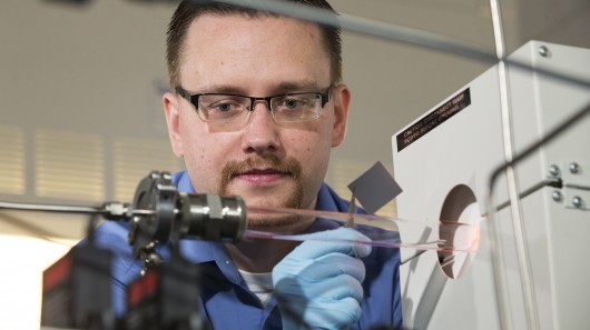
A newly developed silicon supercapacitor could allow for the seamless integration of energy storage and microchips
A team of researchers at the Vanderbilt University in Nashville, Tennessee has designed a supercapacitor made primarily of silicon that has shown much improved power density over its commercially available alternatives. The advance could allow for interesting integration of battery technology in everyday electronics, from solar cells to smartphones.
Supercapacitors store electricity by gathering ions on the surface of two plates soaked in an electrolyte solution. Because the number of ions that can be stored depends on the surface area of the plates, these are usually coated with materials, such as activated carbon, that are highly porous at the nanometric scale.
While supercapacitors can't quite match the energy storage capabilities of lithium-ion batteries, they can absorb and release charge much more rapidly and have a significantly longer lifespan. Today, supercapacitors are used in applications ranging from stabilizing the power supply in portable electronics to supporting the KERS system in Formula 1 cars.
Scientists have tried to improve on the amount of energy that supercapacitors can store by depositing even more porous materials materials such as carbon nanotubes on their plates, but these attempts have only produced marginal improvements that have been hard to replicate consistently.
Assistant professor Cary Pint and his colleagues at Vanderbilt chose to attack the problem from a new and unusual angle by attempting to build a capacitor out of porous silicon.
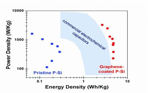
The silicon supercapacitor showed higher energy densities than commercial devices, though they are still a long way from the energy density of lithium-ion batteries
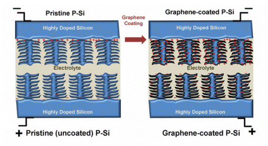
The porous silicon was insulated by coating it with a thin layer of graphene
At first this seemed like an unlikely path, since silicon is known to react strongly with the electrolyte, disrupting the working mechanism of supercapacitors. On the other hand, the electronics industry is very familiar with ways to manipulate silicon precisely and make it highly porous.
Pint and his colleagues coated the porous silicon in carbon and heated the ensemble to about 800° C (1500° F). The process formed a layer of graphene only a few nanometers thick that insulated the silicon from the electrolyte while retaining its highly porous structure.
The researchers found that supercapacitor plates manufactured in this fashion were up to 40 times more energy-dense than those made out of the "naked" silicon, and achieved a performance that significantly improved on current commercial supercapacitors.
Applications
Silicon is the second most abundant element on Earth, and the ability to manufacture supercapacitors from it along with the integrated circuits that it powers could have very interesting repercussions all across the electronics industry.
According to the researchers, it should be possible to build cheap silicon supercapacitors out of the excess silicon contained inside many electronic devices. One such example are solar cells: supercapacitors built out of the silicon in the back side of solar cells could store energy during the day and gradually release it into the energy grid during the hours of peak consumption.
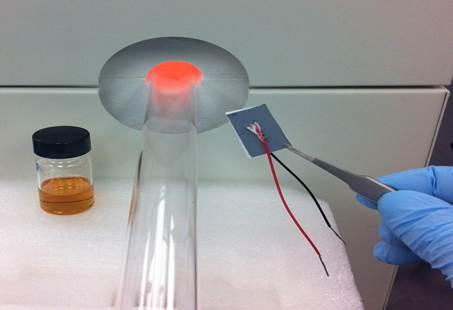
On the left, the electrolyte used in the supercapacitor; in the middle, the furnace that was used to deposit graphene; on the right, a silicon supercapacitor
.
Student Achievements
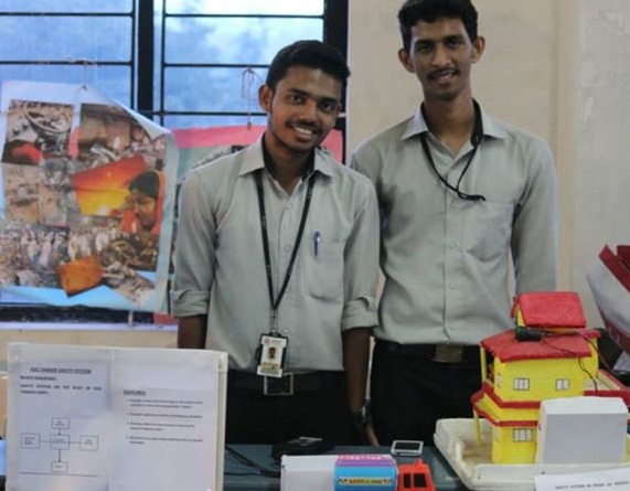
Mukul.S.Yash and Nithin Baby of S7 EC β bagged several achievements for their Mini Project “GAS TANKER SAFETY SYSTEM, For a safe and secure world”. Their project was selected for the National Level Project Innovation Contest “TECHTOP 2013”.They claimed the second position at the National Level Technical Fest “HORIZON ’13” held at St.Git’s College of Engineering, Kottayam. They also bagged the “Visitor’s Choice Award ” and Third Prize in the “Project Expo 2013” held at RSET.
Student Achievements
| S. No. | Name | Event name | Conducted/Organized by | Position secured |
| 1. | Cindy Mathew
|
360 degree (Igniz 2013) | SCMS Engg College | first |
| 2. | Vigneshwer Dhinakaran
|
Extundo Prodigo(excel 2013) | Govt. Model Engineering College | Second |
| 3. | Keerthana S Menon
|
Extrinsicity(excel 2013) | Govt. Model Engineering College | Second |
| 4. | Sneha Paulson
|
Extrinsicity(excel 2013) | Govt. Model Engineering College | Second |
| 5. | Vinaya P Jose
|
Extrinsicity(excel 2013) | Govt. Model Engineering College | Second |


CONGRATULATION!!!
Irene Dias |
We congratulate our student Irene Dias of S5 ECα for her brilliant performance and becoming the Kalathilakam in BHARATHAM 2013. |
Industrial Interaction
Courses given from industry
| 6/04/2013 | Electronics System Design and Manufacturing | Nest,Ark Power Controls Pvt .ltd
|
| 18/05/2013 | Mentor Graphic Tools | Trident Technologies
|
| 19/07/2013 | System on Chip (Soc) Validation and verification | Intel
|
| 26/09/2013-27/09/2013 | 2 Day PIC WORKSHOP | TBI (AIS) Technopark
|
| 27/09/2013-28/09/2013 | 2 Day ARM WORKSHOP | TBI (AIS) Technopark
|


DEPARTMENTAL ACTIVITY
Workshop on Software Defined Radio
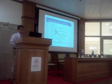
Department of Electronics and Communication of RSET, conducted a Three Day Seminar on Software Defined Radio (SDR) Sponsored by DRDO and Technically supported by IEEE Kochi subsection on 14th,15th and 16th of May 2013. The seminar was intended to impart advanced concepts towards realizing feasible solutions in SDR to PG Students/Faculty/Professionals
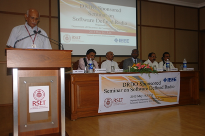
The keynote address was delivered by Prof. R. David Koilpillai, EE Department, IIT Chennai on “Cellular Evolution to 4G - Opportunities for SDR” and “SDR Enabled Cognitive Radio - A Perspective”. The technical sessions were handled by eminent resource persons from organizations like DRDO, CDAC, Amritha University, NIT Calicut, IIST Trivandrum and Industry (National Instruments). Mr. Sameer Babu T. P and Dr P. Murali Krishna from NPOL, Cochin, Mr. Prem Krishnan N, Senior Engineer, CDAC, Trivandrum, Mr. Sagar Yadav, National Instruments (NI), Prof. K. P. Soman, Amrita University, Coimbatore, Dr. S. M. Sameer, NIT Calicut, Dr. Manoj B. S., IIST, Trivandrum handled the technical sessions.
Starting with fundamentals of multi-rate DSP, the course explored digital front end design, timing/frequency synchronization for single and multi carrier systems and efficient channelization strategies. Industry session on NI RF Hardware and USRP were also included.
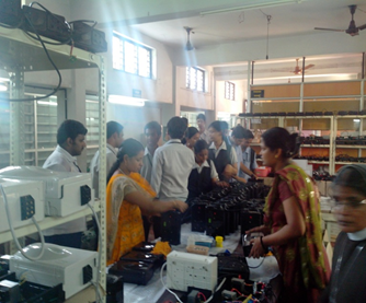
Workshop on ELECTRONIC SYSTEM DESIGN AND MANUFACTURING (ESDM)
Department of Electronics and Communication (DEC) organized a 1 day workshop on Electronic System Design and Manufacturing on 6th April 2013. The workshop was inaugurated by Mrs. Mini Ulanat, faculty in the Post Graduate Department of Computer Science, Cochin University of Science & Technology.
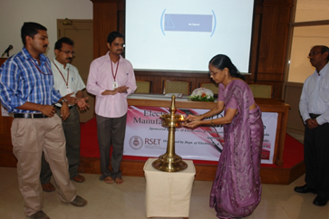
After the inaugural ceremony, Mr. Binu Augustin, Director and Mr. Aneesh Kumar, Asst. Manager of ARK MOTION handled the technical sessions which was followed by a fun and interactive session on ‘Mind 2 Market’ handled by Dr. Suresh Nair, CTO, SFO Technology, NeST, Cochin.
The participants of workshop visited SFO Technology and V-Guard, accompanied by faculties of EC Department.
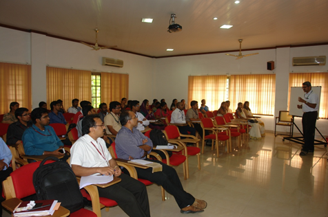
One Day Workshop on Wireless Communication
The Department of Electronics and Communication conducted a one day workshop on 26th October 2013 for the faculty members from different colleges involved with ''Wireless Communications'' course under the MG University M. Tech. Communication Engineering syllabus. The prime motivation of the course was to familiarise the faculty members with the current developments and give an insight into providing sound understanding on fundamental concepts to the students in order to help them build the platform on which current developments can be understood and future contributions can be made. The technical sessions were handled by Prof. (Dr.) A. V. Babu from National Institute Of Technology, Calicut and Prof. (Dr.) Neelakantan P. C. from Adi Shankara School of Engineering and Technology. The workshop presented systematic and organized view on wireless communication systems and technologies.
DEPARTMENTAL ACTIVITY
PROJECT EXPO 2013
Project Expo ’13 is an initiative by the final year students and teachers of Electronics and Communication Engineering Department where the students had an opportunity to exhibit their Mini project . The exhibition started unofficially on August 2nd, 2013 afternoon at PG Hall. 30 groups of students set up their projects which they had developed in their 6th semester. Fr. Antony Kariyil, Director of RSET was the first to visit the project exhibition. The students of the college also visited the exhibition the same day. Project Expo ’13 was officially inaugurated by the Principal of RSET, Dr. J. Isaac On 3rd August, 2013 at 9:30 am.
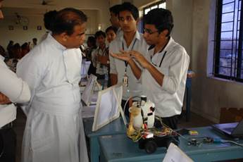
Students from different schools and professionals from Tata Consultancy Services, Unisync Technologies and Rajagiri Centre for Business Studies also visited the exhibition.
Industrial visit 2009-2013
Companies Visited
FCI OEN(Mulanthuruthy)
Indian Telephone Industries(Bangalore)
Keltron Controls (Aroor)
Keltron(Thiruvananthapuram)
Cochin Port Trust,
SFO Technologies Pvt Ltd,
NEST(Kakkanad),
HAL( Bangalore),
National Informatic Centre(CAD group, New Delhi),
Tile Marine LLC(Dubai,UAE),
EtiSalat(Abu Dabi,UAE),
Malayala Manorama(Kottayam )
Student Enterpreneurs
- Akash Mathew (2009-2013 batch)- CEO & Director , CIED Technologies Pvt. Ltd.
His company was Selected as one among the top 5 startup companies to win a pitch contest organised by startup village for getting an investment of 70 Lakhs. He was selected by Kerala Government as one among the top 5 student entrepreneurs who also gets a chance to visit Silicon Valley in an all expense paid trip, sponsored by Govt. of Kerala. The visit will give a chance to the entrepreneurs to meet tech giants like Larry Page ( CEO Google ), Mark Zuckerberg ( CEO Facebook). His company is presently working on three sectors including Industrial automation project , Cloud based apps and Android apps.
- Ashiq Kallingal and Anto Varghese (2009 -2013 batch) – cofounders of Addictive Innovations Pvt. Ltd.
Their products include e-Wall, LetMeKnw and ShopOnLady. Their maiden venture in the field of mobile advertisement, "e-wall", the multipurpose interactive screen was first launched for Bharatham, cultural fest of RSET. This was also used for Ragam, cultural fest of NIT,Calicut.
FACULTY CORNER
Accomplishments:
Paper Publication
Faculty research publication details (DEC)
1.Rooha Razmid Ahamed, Shofia Ram “Comparison & Analysis of Sequential Circuits using Different logic styles”, International Journal of Enhanced Research in Science, Technology & Engineering ,ISSN 2319-7463, Vol.2, Issue 8, August 2013
2.Rooha Razmid Ahmed, Shofia Ram, “Comparison & Analysis of combinational circuits using different logic styles”, Proceedings of 4th IEEE International Conference on Computing, Communication and Networking Technologies (ICCCNT2013) ,July 4-6 ,2013
3.Rony Antony P & Elina Rajan,” Implementation of Extended Open Core Protocol Interface Memory System using Verilog HDL ”, International Conference On Green Computing , Communication And Conservation Of Energy (ICGCE 2013), December 12-14(2013) (Paper Accepted)
4.Jaison Jacob, Babita R Jose, “Decision Fusion in in Co-operative Spectrum Sensing: A Fuzzy Based Approach” Proceedings of International Workshop on Recent advances in Computing and Communications -2013, RSET, August 2013. Pp. 23-26.
5.Jaison Jacob, Babita R Jose, Jimson Mathew ,Cellular Automata Approach for a Low Power Fusion Center to Evaluate Spectrum Status and Coverage Area in Cognitive Radios” Journal of Low Power Electronics, Vol. 9, 1–8, 2013
6.Harsha A, Gopika Gopan, “Adaptive Neuro-Fuzzy Classifier for ‘Petit Mal’Epilepsy Detection using Mean Teager”, 2013 IEEE International Conference on Advances in Computing, Communications and Informatics (ICACCI) ,August 22-25, 978-1-4673-6217-7/13/$31.00_c 2013 IEEE
7.Harsha A, Eldho S Kollilalil, ‘’Single Feature-Based Non-Convulsive Epileptic Seizure Detection using Multi-Class SVM”, 2013 IEEE -C2SPCA October 10-11, 2013 . CFP13SPF-ART ISBN Number 978-1-4799-1085-4.
8.Anoop Thomas& P.A.Silpa, “Implementation of PCA Algorithm on ARM9 for face recognition”, Proceedings of Second National Conference on Emerging Trends in Computing (NCEITC13) ,June 13-15 ,2013(ISBN 978-93-82338-64-2)
9.Anoop Thomas & Praiz Madappillil,” Power Quality Detection Algorithms using moving window Technique” Proceedings of Second National Conference on Emerging Trends in Computing (NCEITC13) ,June 13-15 ,2013(ISBN 978-93-82338-64-2)
10.Anoop Thomas& P.A.Silpa, “Porting of operating system to friendly arm board”, Proceedings of IEEE Third International Conference on Advances in Computing and Communications (ICACCC 2013) , Aug 29 – 31, 2013
11.Anoop Thomas & Lakshmi Santhosh,” Implementation of Radix 2 and Radix 22 FFT Algorithms on Spartan6 FPGA”, Proceedings of 4th IEEE International Conference on Computing, Communication & Networking Technologies (ICCNT), July 4-6 ,2013
12.Tressa Micahel & Catherine Glenitta Figueiredo , “A VLSI architecture for arrhythmia
Detection in biomedical application”, Proceedings of 4th IEEE International Conference on Computing, Communication & Networking Technologies (ICCNT), July 4-6 ,2013
13.Teffi Francis, Treasa Joseph and Jobin K. Antony, “Modified MAC Unit for low power high speed DSP application using multiplier with bypassing technique and optimized adders” IVth IEEE International conference on Computing, commn. and Networking Technologies, Tiruchengode, Tamilnadu (July 2013).
14.Sreekumar G, Aswathy P & N Suresh Kumar “DOA Estimation Using Sparse Planar Vector Sensor Array in Shallow Ocean”, Proceedings of International Symposium on Ocean Electronics (SYMPOL), October 2013.
15.Princy Maria Paul, Priya Annmary C., N. Sneha Mol Treesa, Sherry Ann Sacharias, Savya Joseph and Deepti Das Krishna, "Miniaturization of Square Patch Antenna using ComplementarySplit Ring Resonators ", 2013 Third International Conference on Advances in Computing and Communications, RSET, pp. 122 - 125, Aug 2013.
16.Nimmy Rose, and Deepti Das Krishna, "Design and Implementation of Multi-Channel Parallel Communication over a wide band in Power Line Communication", 4th IEEE international conference on Computing, Communication and Networking Technologies (ICCCNT 2013), July 2013
FACULTY CORNER
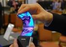
Flexible display
BY :- Bonifus PL , Asistant Professor DEC
A flexible display is a display which is flexible in nature; differentiable from the more prevalent traditional flat screen displays used in most electronics devices. In the recent years there has been a growing interest from numerous consumer electronics manufacturers to apply this display technology in e-readers, mobile phones and other consumer electronics.
Flexible OLEDs
An OLED (organic light-emitting diode) is a light-emitting diode (LED) in which the emissive electroluminescent layer is a film of organic compound which emits light in response to an electric current. This layer of organic semiconductor is situated between two electrodes. Generally, at least one of these electrodes is transparent.
OLED is an emerging display technology that enables beautiful and efficient displays and lighting panels. Thin OLEDs are already being used in many mobile devices and TVs, and the next generation of these panels will be flexible and bendable.
Different kinds of flexibility
When we talk about flexible OLEDs, it's important to understand what that means exactly. A flexible OLED is based on a flexible substrate which can be either plastic, metal or flexible glass. The plastic and metal panels will be light, thin and very durable - in fact they will be virtually shatter-proof.
It is estimated that the first range of devices to use a flexible display won't be flexible at all. While the manufacturer may bend the display or curve it around a non-flat surface, the final user will not be able to actually bend the device. Still it will have several advantages: these displays will be lighter, thinner and much more durable compared to glass based displays.
Second generation flexible OLED devices may indeed be flexible to the final user. Finally, when the technology is ready, we may see OLED panels that you can fold, bend or stretch. This may create all sorts of exciting designs that will enable large displays to be placed in a mobile device and only be opened when required.
Flexible OLED products
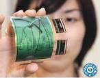
After years of research, in October 2013, Samsung announced the world's first product to use a flexible OLED display - the Galaxy Curve smartphone. This is an Android 4.3 smartphone similar to the Galaxy Note 3, with the major feature being the 5.7" Full-HD curved (400 mm curvature radius) flexible display.
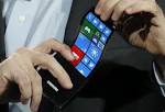
LG is producing flexible OLED panels, 6" in size. It is expected that LG will also unveil their own smartphone G Flex with a flexible OLED towards the end of 2013.
Initial capacity in both companies is low (a few hundreds of thousands of panels per month). Samsung's capacity is higher (they are using a Gen-5.5 line and LG is using a Gen-4.5 line) but this too will not be enough even for a single mass market phone. The companies are probably waiting to see how consumers react to those new panels before they commit to increase capacity.
Samsung launched their YOUM flexible OLED panels in January 2013, showing some cool prototypes of curved and flexible OLED displays.
Some reports suggest that Apple is planning to use a small (about 1.5" in size) flexible OLED panel in their upcoming smart-watch device. This isn't confirmed yet and it will probably be a while before Apple chooses a flexible OLED for a mass market device.
Curved OLED TVs
Both Samsung and LG are now offering curved OLED TVs. These 55" panels are slightly curved and this offers a better viewing experience for someone who sits right in front of the TV as all the pixels are at the same distance from his eyes. Most people however, actually prefer a flat panel. In any case, as far as the OLED panel is concerned this isn't really a flexible OLED, it is a curved glass-based OLED panel.
OLED TV production capacity is extremely low and prices are very high. Samsung's KN55S9C for example costs $8,997 while LG's 55EA9800 is even more expensive at $9,999. Both panels are 55" in size and offer Full-HD resolution. Reviews of those TVs have been spectacular, with all reviewers saying that OLED TVs offer the best picture quality ever.
FACULTY CORNER
New Optical Disc Can Store Information "For A Billion Years"
By:- Abhishek Viswakumar, Asistant Professor DEC
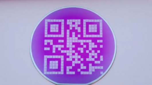
A new optical disc uses QR codes etched in tungsten to achieve extreme levels of heat resistance (Image: de Vries/University of Twente)
A researcher at the University of Twente in the Netherlands has developed a new optical memory device out of tungsten and silicon nitride that he says could store data safely for extremely long periods of time – up to a billion years.
Hard drives are very susceptible to external magnetic fields and mechanical failures, with a normal lifespan not much longer than 10 years; similarly CDs, DVDs and flash drives each have their own Achilles' heel.
University of Twente researcher Jeroen de Vries set out to solve this problem by designing his own data storing device. For the materials he chose tungsten, which can withstand very high temperatures, encapsulated in silicon nitride, which is highly resistant to fracture and deforms very little when exposed to high levels of heat.
The disc, de Vries claims, is so sturdy that it could be used to store important data on the human race and retain it well past its extinction, for the benefit of whoever is left (of course, that's assuming that the aliens, robots, or mutants will somehow know exactly how to decode the information on the disk in the first place).
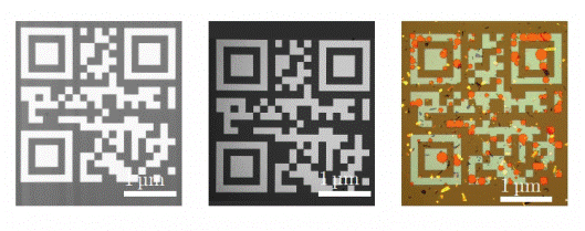
From left to right: the QR codes after fabrication, after two hours at 613 K, and after two hours at 763 K (Image: de Vries/University of Twente)
Inside the device, information is stored by etching QR codes in tungsten – which can be easily decoded by today's smartphones. This method is very resilient because the information is still preserved even when up to seven percent of the data has been compromised. Each pixel of the code also has within it a second set of much smaller QR codes, with pixels of only a few microns in size.
To find out how long the device could retain information, de Vries relied on the Arrhenius model, which simulates extended periods of time by exposing the device to predetermined levels of heat for a set amount of time.
The researcher heated the storage device to a temperature of 200 °C (400 °F) for one hour and noted no visible degradation, which according to the model simulates one million years of usage. The device only showed some signs of degradation once it was heated to much higher temperatures, around 440 °C (820 °F) – but even then, the tungsten was not harmed and the data was still readable.
Though the mathematical model used for testing was limited to exposure to high temperatures (and, as the researcher admits, may not be entirely accurate), de Vries says that if they can find a place that is very stable to store the device, such as a nuclear storage facility, then the disc and the data it contains still has all the requisites to last for extremely long periods of time, on the order of millions of years.
FACULTY CORNER
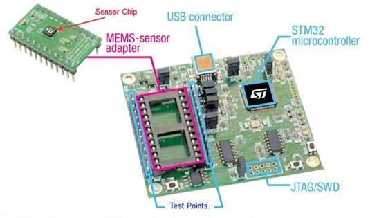
Smallest commercial electronic compass chip is dwarfed by a grain of rice
By :- Dhanesh M S, Asistant Professor DEC
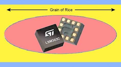
The tiny eCompass chip provides magnetometer and accelerometer capabilities
STMicroelectronics has announced a new MEMS-based module that integrates a three-axis magnetometer, a three-axis accelerometer, A/D converters, and control logic on a 2 mm x 2 mm x 1 mm surface mount chip, reportedly making it the smallest electronic compass available today.
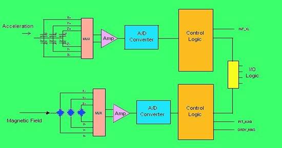
Block diagram of eCompass chip
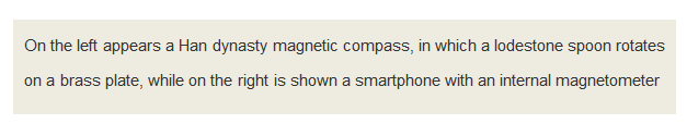
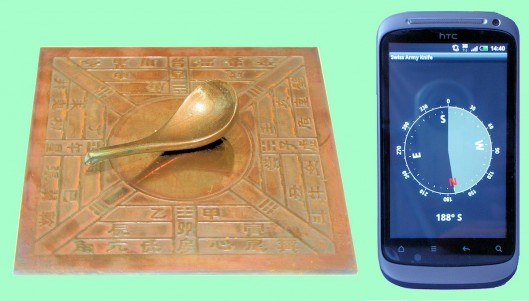
Magnetic compasses were first invented during the Han dynasty in China about 200 BC. These compasses were based on observing a permanent magnet align itself to the Earth's magnetic field, and are still used today, albeit in dramatically evolved forms.
LSM303C eCompass The advent of portable personal electronics has opened a commercial niche for new varieties of compasses that are easily integrated to digital systems. In recent years, the trend has been to measure the Earth's magnetic field using anisotropic magnetoresistance sensors, which are used in STMicroelectronics' new LSM303C eCompass chip. The electrical resistance of such sensors depends on the angle between the current flow and the magnetic field within a permalloy film. The three AMR magnetometers (x, y, and z-axis) in the LSM303C chip can measure magnetic fields of +16 gauss with a resolution of less than a milligauss.
What are accelerometers doing on a compass chip? The magnetometers can determine the magnitude and orientation of the Earth's magnetic field relative to portable devices like smartphones, but navigation requires that you know the orientation of the field relative to the Earth's surface. The three-axis accelerometers are used to measure the angular difference between the xy plane of the magnetometers and the xy plane of the Earth's surface, allowing the smartphone to calculate the orientation of the local magnetic field relative to the Earth's surface so it can point north.
That all this capability can be commercially fabricated in four cubic millimeters requiring less than a milliwatt of power is rather astounding, and indicates the rapid advance in miniaturizing sensor packages. With the addition of a three-axis MEMS gyroscope, this chip would form the heart of an inertial guidance system, a useful tool for avoiding getting lost on a hike through the woods.
FACULTY CORNER
Medical Applications of Ultra-WideBand (UWB)
BY:- Harsha .A, Assistant Professor DEC
As an emerging technology, Ultra Wide Band (UWB) wireless communications provides a very different approach to wireless technologies compared to conventional narrow band systems, which brings huge research interests in it. Because of this, UWB has many potential applications to be researched. One of the promising application areas is in medicine. Some unique features of UWB make it very suitable for medical areas.
Ultra-wideband (UWB) radio is an emerging technology with some unique attractive features which are combined with researches in other fields such as wireless ommunications, radar, and medical engineering fields. Formally before 2001, UWB's application is limited mainly in military areas. However, since 2002, FCC has gradually allowed the commercial usage of these bandwidths, which makes it possible that every common people could benefit the UWB features. Federal Communications Commission (FCC) regulate that the frequency for the UWB technique is from 3.1GHz to 10.6GHz in America . However, in Europe , the frequencies include two parts: from 3.4 GHz to 4.8 GHz and 6 GHz to 8.5 GHz. The power radiation requirement of UWB is strict and it would not disturb the existing equipments because UWB's spectrum looks like background noise.
UWB features for Medical Application
1. Penetrating through obstacles
2. High precision ranging at the centimeter level
3. Low electromagnetic radiation
4. Low processing energy consumed
One of the key medical application of UWB is medical imaging. The four main subsections are Cardiology Imaging, Pneumology Imaging, Obstetrics Imaging, and Ear-Nose-Throat Imaging.
Cardiology Imaging
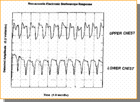
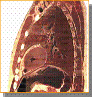
This is one of the Actually, the first applications using UWB radar technology was for heart monitoring since the heart related research has a high impact on general public. Figure below shows
the radar stethoscope to monitor the heart movement
.

The UWB radar is able to detect, non-invasively, 7 of 12 movements of heart which is shown
Below Heart imaging using UWB
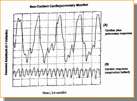
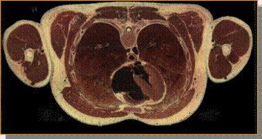
UWB transmitter emits discrete pulses to the human body and the reflected pulses from the heart arrived at UWBreceiver and then the result is recorded. Signal processing is performed through obtaining the pulses response. For example, there exists a definite difference in reflection magnitude between the heart muscle and the blood when detecting the heart wall by UWB radar. Because of the impedance difference between the cardiac muscle and blood,
a roughly 10% reflection magnitude of the radio frequency energy at the heart muscle-blood boundary can be expected. The UWB receiver can measure the difference, and show it on the screen, which reflects the status of heart.
Other medical application areas of UWB
• Underwater medicine measurements.
• Space medicine measurements.
• Sport medicine measurements.
• Military medicine.
• Emergency medicine: Rubble Rescue Radar
Research Directions
Future research studies in the medical domain to correlate UWB include:
• ultrasound heart M-Mode tracings.
• external phonocardiogram and apexcardiogram tracings.
• external ballistocardiogram tracings.
• invasive pressure pulse recordings.
• electrocardiogram recordings.
• better understanding and modeling of RF pulse propagation in the living tissues